

Hardwired AI chips and inference economics: silicon optimization for cheap, ubiquitous models
The world of artificial intelligence is changing rapidly as we move toward hardwired AI chips. Traditional hardware often struggles with the high costs of running large language models. Consequently, researchers are turning to silicon optimization to make intelligence affordable for everyone. This shift marks a transition from general purpose computing to specialized hardware architectures.
We need AI to be as common as plastic in our daily lives. However, current systems rely on expensive power hungry GPUs that limit accessibility. Hardwired AI chips solve this problem by etching model weights directly into the silicon. As a result, inference becomes faster and significantly cheaper than ever before.
This article explores how direct to silicon designs redefine the unit economics of AI. Furthermore, we look at how startups like Taalas challenge the dominance of giants like NVIDIA. You will learn why specialized inference chips are the future of AI infrastructure. Because efficiency is now the priority, silicon optimization is no longer optional.
The current memory wall creates a bottleneck for traditional processors. Therefore, engineers are building Application Specific Integrated Circuits to bypass these limits. These designs offer a path toward cheap and ubiquitous models for every industry. This evolution ensures that AI power is no longer restricted to massive data centers.
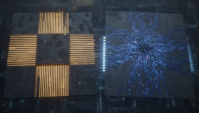
Visual Concept: AI Silicon Evolution
A glowing silicon chip at the center of the frame transforms into liquid light. These light streams flow outward like digital rivers representing fast and efficient data streams. The transition from solid hardware to fluid intelligence highlights the speed of modern silicon optimization.
Understanding the Mechanics of Hardwired AI Chips
Standard artificial intelligence runs on flexible but inefficient hardware. Most current systems utilize programmable GPUs to handle complex mathematical operations. While these units are versatile, they often struggle with the specific demands of a large language model. Hardwired AI chips offer a much more efficient alternative for modern workloads. This shift toward specialized hardware represents a massive leap in computing power.
The Technical Architecture of Hardwired AI Chips
Specialized hardware changes how we process data. Startups such as Taalas are pioneering a new approach to silicon. In their HC1 (Hardcore 1) chip, the model’s weights and architecture are literally etched into the wiring of the silicon. This method removes the layers of software that usually slow down processing. Because the logic is physical, the chip does not need to fetch instructions constantly.
Efficiency improves when we remove the overhead of general purpose computing:
- Standard GPUs rely on broad software instructions.
- Hardwired silicon designs focus on one specific task.
- Traditional infrastructure hits a performance ceiling called the memory wall.
- Direct to silicon etching allows for much higher throughput.
The Technical Edge of Hardwired AI Chips
Silicon optimization is the key to cheaper intelligence. Traditional AI infrastructure requires massive amounts of energy to maintain flexibility. For example, a traditional GPU might serve a single user at approximately 150 tokens per second. However, hardwired AI chips like the HC1 achieve between 16,000 to 17,000 tokens per second. As a result, these chips can deliver results at a fraction of the cost.
Therefore, companies can deploy massive models without the usual financial burden. This shift moves the industry away from generic hardware produced by companies like NVIDIA. Furthermore, this transition ensures that AI becomes a truly ubiquitous resource. Taalas can even generate a chip design in roughly a week and manufacture it in two months. Consequently, custom Application Specific Integrated Circuit designs are now accessible for specific AI needs. Using specialized inference chips is the fastest way to scale global intelligence.
Performance Comparison of Hardwired AI Chips
Comparing different hardware types clarifies the benefits of silicon optimization for the entire industry. Many companies rely on programmable GPUs because they offer flexibility for various mathematical tasks across different platforms. However, specialized inference chips prioritize efficiency over versatility in specific high performance environments.
This table highlights how hardwired AI chips perform against current industry hardware standards in real world applications. Because operational costs are rising, businesses must evaluate their infrastructure choices more carefully than before. Furthermore, the shift toward direct to silicon designs is gaining momentum among global tech leaders.
Efficiency Metrics for Hardwired AI Chips
| Feature | Hardwired AI Chips (Taalas HC1) | Programmable GPUs (NVIDIA H100) |
|---|---|---|
| Performance (token per second) | 16,000 to 17,000 | Approximately 150 |
| Architecture Type | ASIC (Application Specific Integrated Circuit) | General Purpose GPU |
| Manufacturing Time | Two months (design in one week) | Standard mass production cycles |
| Optimization Method | Direct to silicon etching | Software simulation of models |
| Scalability | High for specific inference tasks | Broad for training and inference |
| Unit Economics | Significantly cheaper for scale | High cost per token |
Analyzing the Impact of Specialized Hardware
The data shows a clear advantage for hardwired AI chips in specific inference tasks. While standard chips handle different types of math, the HC1 focuses purely on model execution logic. Consequently, the throughput for every token per second is much higher than generic processors found in modern data centers.
This efficiency reduces the total cost of ownership for large scale digital deployments across multiple regions. As a result, companies can scale their intelligence without increasing their energy budgets or environmental impact. Additionally, using an ASIC approach ensures that hardware performance matches specific software requirements perfectly. Companies like Taalas and NVIDIA continue to push the boundaries of what is possible in this space.
The Impact of Hardwired AI Chips on Inference Economics
The economics of artificial intelligence depend heavily on hardware performance. Current AI infrastructure often relies on general purpose processors that process data slowly. However hardwired AI chips are changing this financial reality by providing massive speed increases. When hardware handles specific model weights directly the efficiency of inference grows exponentially. This shift leads to a dramatic reduction in the cost of generating digital intelligence.
- High throughput reduces the cost for every single token.
- Direct designs eliminate unnecessary energy waste during processing.
- Specialized silicon allows companies to run larger models on smaller budgets.
Transforming Unit Economics in AI Infrastructure
The unit economics of running a large language model on a traditional GPU are often prohibitive. For instance a standard processor might serve a single user at 150 tokens per second. In contrast the HC1 chip from Taalas reaches between 16000 to 17000 tokens per second. Therefore the price per token drops by several orders of magnitude. This change makes it possible for smaller firms to compete with tech giants.
Silicon optimization allows developers to bypass the traditional memory wall. Because the model architecture is etched into the chip data does not need to travel far. Consequently the power requirements for complex tasks decrease significantly. This efficiency is essential for creating ubiquitous models that run on every device. As a result we see a future where intelligence is as affordable as electricity.
Building a custom chip used to take years of development time. However Taalas can now generate a design in just one week. Furthermore the manufacturing process only takes two months to complete. This rapid turnaround time accelerates the deployment of specialized inference chips across the globe. Therefore the barriers to entry for custom AI hardware are falling quickly. Business leaders must recognize these shifts to remain competitive in the digital market.
More information about these trends is available at Forbes and CNBC.
The Future of AI Infrastructure and Economic Growth
The rise of hardwired AI chips marks a new era for hardware efficiency. These processors change the fundamental rules of AI inference economics. By casting logic into silicon, companies can achieve incredible performance gains. Consequently, the total cost for running large models will drop significantly. Furthermore, this shift makes intelligence accessible for every industry across the globe.
Employee Number Zero LLC helps businesses navigate this complex technical world. This US-based firm provides expert AI and automation solutions for growth. Because they focus on sales and marketing automation tools, they drive real results. Their team operates as a full stack brand trained AI worker for your organization. As a result, you can multiply revenue using advanced growth systems.
Security remains a top priority for modern digital infrastructure. Employee Number Zero LLC ensures every system is securely deployed under client control. Therefore, you maintain data privacy while leveraging the power of automation. Moreover, their solutions are designed to scale with your business needs effortlessly. You can read their latest technical insights on their blog at Employee Number Zero Blog for more information.
The combination of hardwired AI chips and expert automation creates a powerful future. Specialized silicon reduces the barriers to entry for advanced intelligence. Soon, complex models will be affordable and ubiquitous for everyone. This evolution ensures that AI power is no longer restricted to massive data centers. We look forward to a world driven by efficient and sustainable digital intelligence.
Frequently Asked Questions about Hardwired AI Chips
What makes hardwired AI chips different from traditional GPUs?
Hardwired AI chips use a specialized design known as an ASIC. Unlike general purpose units these chips have specific logic paths etched into the silicon. Standard programmable GPUs must simulate intelligence through complex software layers.
However hardwired chips cast the model weights directly into the physical wiring. This architecture removes the overhead that usually slows down digital processing. As a result the hardware runs specific AI models with much higher efficiency.
Why do hardwired AI chips improve the economics of inference?
The cost of running a model depends on how many tokens a chip can process per second. Traditional hardware might only handle around 150 tokens per second for a single user. In contrast hardwired AI chips like the HC1 reach up to 17000 tokens per second.
This massive increase in speed allows companies to serve more users with less hardware. Because the energy consumption also drops the total cost of ownership becomes much lower. Consequently businesses can scale their operations without spending huge sums on electricity.
How does silicon optimization solve the problem of the memory wall?
The memory wall occurs when data cannot move fast enough between the processor and storage. Traditional systems waste energy moving information across long digital paths. Silicon optimization solves this by placing the model weights directly on the chip circuits.
Data travels much shorter distances within the hardwired AI chips. This design significantly reduces latency during the inference process. Therefore the entire system operates at peak performance without hitting traditional bottlenecks. It is a fundamental shift in how we build AI infrastructure.
Is the manufacturing process for these specialized chips slow?
Creating a custom chip used to take years of research and development. However modern automated design flows have changed the timeline for production. Startups like Taalas can now generate a full chip design in roughly one week.
The actual manufacturing of the silicon takes about two months to complete. This rapid cycle allows companies to deploy specialized inference chips very quickly. As a result the industry can keep up with the fast pace of software innovation. Rapid production makes custom hardware a viable option for many firms.
Will hardwired AI chips make AI models ubiquitous?
Yes these chips are essential for making intelligence cheap and common everywhere. High costs currently prevent many organizations from using large scale models. When hardware becomes more efficient the price of intelligence drops toward zero.
This change enables the integration of advanced logic into every digital device. Hardwired AI chips provide the power needed for offline or edge computing. Because the chips are small and efficient they fit into various consumer products. This transition ensures that AI becomes a truly ubiquitous resource for everyone.